Short answer
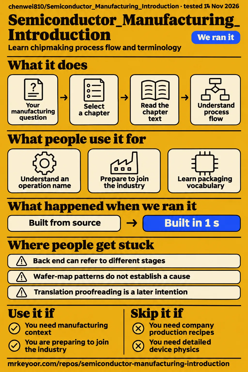
Semiconductor_Manufacturing_Introduction is a beginner book about chipmaking process flow and terminology. It suits software and firmware engineers who need manufacturing context, newcomers preparing to join the industry, and readers placing packaging or test within the wider process. Choose another resource for company production recipes, detailed device-physics derivations or unrestricted commercial reuse. Those distinctions follow the author's stated scope and license and give a clearer selection rule than the repository's Python classification.
The book follows a wafer from material preparation through fabrication, testing and packaging. Its project README and contents connect that journey to numbered chapters and role-specific routes. Chapter 11 is a useful sample because it joins individual manufacturing operations into a CMOS flow. Read its explanation of transistor formation, contacts and wiring, then decide whether that level of detail matches the conversations you need to follow at work.
What you can do with Semiconductor_Manufacturing_Introduction
The README provides four reading routes: a quick overview, software and firmware context, industry entry, and packaging and test. Each route selects chapters according to a reader's immediate purpose. The introductory route connects fab organization with process integration and node terminology; the software route adds transistor basics, memory, reliability, factory systems and firmware. Keep this table as the chapter-selection reference rather than treating every chapter as a prerequisite for every reader.
| Your immediate job | The README's reading path | What to look for while reading |
|---|---|---|
| Get oriented | Chapters 0, 1, 11, 14 | Connect fab organization, process flow and process-node terminology |
| Understand manufacturing context for software or firmware | Chapters 0, 2, 11, 13, 14, 22, 23, 24 | Connect transistors and memory with systems and firmware |
| Prepare to join the industry | Whole book, especially 1, 11, 15 through 18 and Appendix B | Learn quality vocabulary alongside process names |
| Work around packaging and test | Chapters 0, 11, 19 through 22 | Place wafer test, packaging and final test within the journey |
These routes come from the author's reading-path table. The contents list chapters 0 through 24 across Parts 0 through 6, followed by three appendices. Including the introductory chapter and part gives 25 numbered chapters and seven parts. That count also explains why a summary that starts counting at chapter 1 can give a different impression of the book's size.
What people use Semiconductor_Manufacturing_Introduction for
Use the book for manufacturing orientation, software and firmware context, industry onboarding, or packaging and test vocabulary. These are learning uses proposed by the README and supplied project descriptions. They give readers concrete reasons to select a chapter: understand an operation name, place a manufacturing stage in sequence, or connect a process topic to their existing role. The translation discussion adds evidence of contribution work around the material.
- The project's orientation route selects the overview, fab organization, CMOS flow and process-node chapters.
- The software and firmware route connects manufacturing topics with memory, systems and firmware.
- The packaging and test route places wafer test, packaging and final test after the process overview.
Issue #2's translation contribution reports an initial Traditional-to-Simplified conversion and adjustments to mainland semiconductor terminology. The contributor names changes for transistor, lithography and die, and the maintainer welcomes submission. That thread describes a practical localization task: selecting regional technical vocabulary as well as converting characters. Its examples help bilingual readers understand why the same manufacturing concept may appear under different terms in different editions.
Repolode's project summary repeats the proposed learning uses, while Hysen Labs' description identifies engineers joining semiconductor teams, hardware developers and students seeking vocabulary. Read those descriptions as recommendations from those pages. The primary README remains the source for choosing chapters, and the sampled chapter text shows what readers encounter after making that choice.
What happened when we ran it
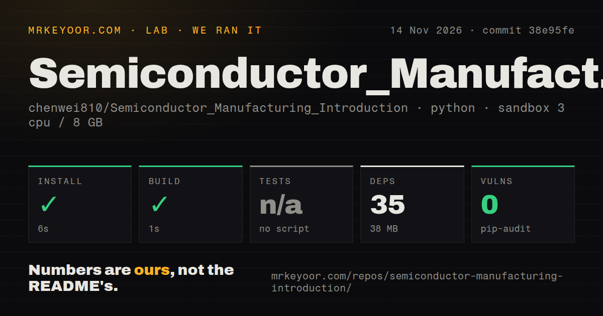
Our November 14, 2026 sandbox run used commit 38e95fe; installation took 6 seconds and the build took 1 second. The recorded configuration had 3 CPUs and 8 GB RAM, with image label ghcr.io/astral-sh/uv:python3.12-bookworm. These are our repository-tooling measurements. The checkout contained 213 files, about 738 source lines and 2 MB of material, and the harness completed its recorded install and build steps.
| Recorded check | Result | What the result means for this review |
|---|---|---|
| Installation | Succeeded in 6 seconds | The recorded dependency-install step completed |
| Dependency inventory | 35 dependencies, 38 MB on disk | The measured environment footprint concerns tooling |
| Build | Succeeded in 1 second | The recorded build step completed |
| Tests | Skipped: no tests script or target | The harness recorded a skipped test step |
| pip-audit | 0 known vulnerabilities | The recorded audit found no known advisories |
| Repository scan | 213 files, about 738 source lines, 2 MB checked out | These metrics describe the checkout |
| Repository signals | 1 CI workflow, no Dockerfile, no tests directory | These are repository scan findings |
We recorded 35 dependencies occupying 38 MB. That footprint matters when investigating the repository's tooling; reading the book uses the Markdown chapter links in the project's English edition. Open a chapter in a browser to assess the material. A dependency installation or build result answers a different question from whether an explanation helps a reader understand manufacturing vocabulary.
A separate November 15 attempt stopped at the failed Compose prerequisite. The record names compose.yaml, compose.yml, docker-compose.yaml and docker-compose.yml as absent and says the harness required a Compose file. The run header nevertheless describes deployment with the repository's own Compose configuration and every port bound to 127.0.0.1. The failed prerequisite contradicts that success wording. The supported outcome is a blocked deployment attempt, followed by teardown marked OK.
Where people get stuck: choosing the right depth
Chapter 11 distinguishes BEOL wiring inside the fab from the back end of packaging and test. That distinction helps newcomers interpret a phrase that can refer to different stages. The chapter groups transistor formation, contacts and wiring into FEOL, MOL and BEOL, then connects those stages through a simplified planar flow. Readers get a sequence of operations and purposes rather than an isolated glossary of manufacturing names.
| Point of confusion | What the source provides | Useful next move |
|---|---|---|
| Treating a reading task as a software deployment task | README links to chapter text; the run records describe tooling | Select the chapter that answers the manufacturing question |
| Treating every use of back end as packaging | Chapter 11 separates BEOL wiring from packaging and test | Establish which stage the speaker means |
| Treating a wafer-map shape as a diagnosis | Chapter 16 pairs patterns with investigation directions and describes physical failure analysis | Separate the observed pattern from its suspected cause |
| Treating the translation thread as completed proofreading | Issue #2 describes proofreading as a later intention | Read the contributor's stated scope and next steps |
Chapter 11's CMOS process flow repeats deposition, lithography, etching or implantation, cleaning and measurement. Its terminology box explains that FEOL builds transistors, MOL connects them to wiring above, and BEOL builds multilevel wiring. The chapter also describes wafers returning to the same kinds of tools during fabrication, connecting the manufacturing sequence to the later discussion of factory systems and scheduling.
Chapter 16's yield and failure analysis explanation separates line yield, die yield and final-test yield. It pairs wafer-map patterns with likely investigation directions, including masks and exposure conditions when failures recur at the same position in every exposure field. Its physical failure-analysis section then describes electrical isolation, deprocessing, cross-sectioning and observation. As a reading exercise, explain the stage, observed pattern and suspected cause separately.
English is a translation of the Traditional Chinese original
The README identifies Traditional Chinese as the original and links English, Simplified Chinese, Japanese and Korean translations. The supplied English samples cover wafer preparation, CMOS integration and yield analysis. Each offers a different entry point: material preparation before fabrication, the sequence inside the fab, or analysis after electrical testing. The README's edition links keep those language choices together at the project's entry page.
The contribution in issue #2 concerns Simplified Chinese and gives concrete examples of regional terminology choices. For a bilingual reading session, compare the relevant passage with the terms your team already uses. The contributor's examples make that task specific: the discussion concerns names for transistors, lithography and dies, rather than a general promise that converting characters alone resolves technical language differences.
Reuse comes with a non-commercial condition
The text and images are licensed under CC BY-NC-SA 4.0. The README describes non-commercial sharing, adaptation and translation with credit and the same license. The primary LICENSE file names the Creative Commons Attribution-NonCommercial-ShareAlike 4.0 International License and supplies its full terms. Use that named license when evaluating redistribution or adaptation, rather than relying on a directory's generic license classification.
A chapter link and a republished illustration involve different actions, so describe your proposed use before applying the terms. The license grants reproduction and sharing for non-commercial purposes under its conditions and separately addresses exceptions and limitations. Its definition of NonCommercial concerns commercial advantage or monetary compensation. For a commercial training product, start with the actual grant and any additional permission your proposed use requires.
Semiconductor_Manufacturing_Introduction vs ASML explainers and SEMI training
ASML introduces six manufacturing steps, SEMI lists virtual instruction, and Semiconductor_Manufacturing_Introduction supplies a chapter-based book. These formats suit different immediate learning tasks. A manufacturer article gives a compact introduction to operation names; the book lets readers select a process or role-specific chapter; a scheduled workshop requires attendance. The comparison below follows their documented format and subject matter rather than assigning them unsupported learning-performance scores.
| Resource | Evidence for its format and scope | Pick it when |
|---|---|---|
| Semiconductor_Manufacturing_Introduction | README: wafer journey, chapter reading paths and language editions | You want selected topics to read at your own pace |
| ASML manufacturing explainer | ASML discusses deposition, photoresist, lithography, etch, ionization and packaging | You need a compact introduction before a longer book |
| SEMI Silicon to Systems | SEMI lists virtual training and live attendance requirements | You want scheduled instruction and can attend |
ASML's explainer discusses six semiconductor manufacturing steps: deposition, photoresist, lithography, etch, ionization and packaging. The ASML article provides that compact organizing list, while the book's contents also name dedicated chapters on cleaning, metrology, process control and firmware context. A reader can use the overview to identify an unfamiliar operation, then select a book chapter when the next question concerns its place in the manufacturing sequence.
SEMI says its virtual training will not be recorded and attendees must be present. The SEMI workshop listing also explains that the registered attendee receives a training link and email reminders. Attendance therefore matters when choosing this format across time zones. The listing names lithography, etching, deposition and CMP among its topics, giving readers concrete subject overlap to compare with the book's contents.
The supplied manufacturing lecture transcript describes earlier coverage of semiconductor materials, intrinsic and extrinsic semiconductors, and devices. The book's README instead emphasizes process flow and deliberately skips heavy physics. That difference helps a reader choose an entry point according to the question at hand: manufacturing vocabulary and sequence, or a course that first develops material and device concepts.
What the other reviews get wrong
The project's LICENSE names CC BY-NC-SA 4.0, which is more useful for reuse decisions than Repolode's generic Other label. The supplied research synthesis identifies that label in Repolode's FAQ, while its project description names the Creative Commons license. Follow the project's complete license and its conditions when deciding whether to share or adapt the text or images.
Hysen Labs' October 18, 2026 push statement is stale relative to the supplied October 30 API observation. The supplied research synthesis records the older statement; the Hysen Labs excerpt dates its editorial analysis October 20 and its metadata snapshot November 14. Those dates describe different parts of the page. The newer snapshot alone does not show that the older editorial sentence received a fresh check. The repository API observation supplies the October 30 pushed_at field.
The primary contents list 25 numbered chapters and seven parts, including chapter 0 and Part 0. GitHub Locker describes 24 chapters and seven parts, Repolode says six parts, and Hysen Labs says 25 chapters. Counting the actual chapter and part labels in the project contents resolves the discrepancy without treating a directory summary as the authority.
The supplied research synthesis also flags ASML's 175-layer NAND example against a CRS passage describing advanced NAND flash chips with over 200 layers. That comparison concerns the background explainer, rather than a measured result for this book. Its useful editorial consequence is narrow: retain ASML's article as an introduction to manufacturing operations and avoid turning its layer-count example into a current upper bound.
Questions people ask
The README says no semiconductor physics background is needed, and its contents organize a structured book rather than a collection of links. Those facts answer two selection questions found in the supplied directory FAQs. The questions below retain the supplied reader intents while keeping chapter selection, edition details and reuse terms in their dedicated sections. Each answer points to the evidence most directly relevant to that particular question.
Do I need a semiconductor physics background to read the book?
No: the README explicitly says no semiconductor physics background is needed. It describes an emphasis on process flow, terminology and fab know-how while skipping heavy physics. That makes the author's introduction the relevant scope statement for a first-time reader. Someone seeking mathematical device-physics instruction should choose material built around that subject rather than expecting this process-oriented introduction to supply it.
What is Semiconductor_Manufacturing_Introduction, and is it a textbook or a collection of links?
It is a structured book with numbered chapters and three appendices. The supplied English chapters contain explanatory prose, terminology boxes and practical notes, not just references to external material. For a representative sample, Chapter 11 joins manufacturing modules into a CMOS flow and explains what FEOL, MOL and BEOL do. That passage shows the teaching format behind the contents list.
Does the book use real company process data?
No: the README says the book uses public information and general industry knowledge and excludes confidential information, company process parameters and internal procedures. It also describes most numbers as approximate values or orders of magnitude. The project disclaimer makes the distinction explicit: this is introductory manufacturing context, and actual values vary by process, product and company.
Is Semiconductor_Manufacturing_Introduction still maintained?
The supplied repository API records a push on October 30, 2026, and issue #2 contains a maintainer reply welcoming translation work. These are concrete activity signals in the supplied evidence. The repository metadata supplies the push timestamp, while the translation discussion supplies the exchange. They answer the dated activity question more precisely than an undated assurance that the project is maintained.
How does sand become a silicon wafer?
Chapter 3 describes purification into polysilicon, growth of a single-crystal ingot, then slicing, lapping, etching, polishing and inspection. The sand-to-wafer chapter also distinguishes single-crystal material from polysilicon and says fabs usually buy wafers from specialized suppliers. Read it when material preparation is the unfamiliar stage, before following the wafer into the circuit-building operations described by later chapters.
What we have not tested yet
Our sandbox results cover repository tooling, and the supplied record contains no learner study, new-hire reading assignment or observed diagnosis of an actual yield problem. The chapter exercise above is a proposed discussion task, not a completed experiment. Hysen Labs' fortnight assessment and provider learning objectives supply no measured learning result for this review. The evidence also contains no controlled comparison of reader outcomes between the book, SEMI instruction and manufacturer explainers.
The supplied English chapters, contents and license support the reading guidance but do not constitute a technical peer review of every chapter. Translation accuracy, professional proofreading, synchronization between editions and translation-script behavior remain unassessed. Issue #2 describes professional proofreading as a later intention. The thread's closed status, the available editions and the maintainer's welcome do not establish that this quality review was completed.
The source-run summary omits command lines and raw toolchain logs, so the recorded image label does not establish actual runtime or operating-system versions. The successful build and zero-known-vulnerability audit do not certify teaching accuracy or future dependency health. The separate deployment attempt has a failed Compose prerequisite and contradictory success header. It supplies no completed task results, hands-on question results or screenshot records.
The supplied video concerns semiconductor education rather than demonstrated use of this repository. Independent learner accounts, search demand, future support and maintenance expectations are unknown. Rendered layout, resolved links, automatic related links, recommendation modules and template content also remain untested. The unassessed score cards reflect the missing contributor-workflow, instructional-quality, support-capacity and maturity evidence; repository activity alone is too narrow a basis for numerical ratings.
Before adding the book to an onboarding checklist, choose one conversation a new colleague needs to follow and discuss the corresponding passage together. Chapter 11's distinction between wiring inside the fab and packaging/test offers a specific starting point. Ask the reader to explain which stage a term refers to and what the operation accomplishes. That proposed next step gives a team a concrete passage to assess without promising an unmeasured learning outcome.